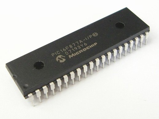
The PIC microcontroller PIC16f877a is one of the most renowned microcontrollers in the industry. This microcontroller is very convenient to use, the coding or programming of this controller is also easier. One of the main advantages is that it can be write-erase as many times as possible because it uses FLASH memory technology. It has a total number of 40 pins and there are 33 pins for input and output. PIC16F877A is used in many pic microcontroller projects. PIC16F877A also have much application in digital electronics circuits.
PIC16f877a finds its applications in a huge number of devices. It is used in remote sensors, security and safety devices, home automation and many industrial instruments. An EEPROM is also featured in it which makes it possible to store some of the information permanently like transmitter codes and receiver frequencies and some other related data. The cost of this controller is low and its handling is also easy. It is flexible and can be used in areas where microcontrollers have never been used before as in microprocessor applications and timer functions etc.
- It has a smaller 35 instructions set.
- It can operate up to 20MHz frequency.
- The operating voltage is between 4.2 volts to 5.5 volts. If you provide it voltage more than 5.5 volts, it may get damaged permanently.
- It does not have an internal oscillator like other PIC18F46K22, PIC18F4550.
- The maximum current each PORT can sink or source is around 100mA. Therefore, the current limit for each GPIO pin of PIC16F877A is 10 mili ampere.
- It is available in four IC packaging such as 40-pin PDIP 44-pin PLCC, 44-pin TQFP, 44-pin QFN
Table of Contents
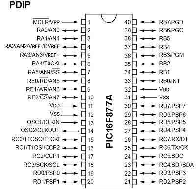
PIN CONFIGURATION AND DESCRIPTION Of PIC16F877A microcontroller- As it has been mentioned before, there are 40 pins of this microcontroller IC. It consists of two 8 bit and one 16 bit timer. Capture and compare modules, serial ports, parallel ports and five input/output ports are also present in it. This picture shows the pinout diagram of PIC16F877A.
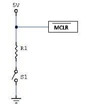
- PIN 1: MCLR:The first pin is the master clear pin of this IC. It resets the microcontroller and is active low, meaning that it should constantly be given a voltage of 5V and if 0 V are given then the controller is reset. Resetting the controller will bring it back to the first line of the program that has been burned into the IC.
- A push button and a resistor is connected to the pin. The pin is already being supplied by constant 5V. When we want to reset the IC we just have to push the button which will bring the MCLR pin to 0 potential thereby resetting the controller.
- PIN 2: RA0/AN0:PORTA consists of 6 pins, from pin 2 to pin 7, all of these are bidirectional input/output pins. Pin 2 is the first pin of this port. This pin can also be used as an analog pin AN0. It is built in analog to digital converter.
- PIN 3: RA1/AN1:This can be the analog input 1.
- PIN 4: RA2/AN2/Vref- :It can also act as the analog input2. Or negative analog reference voltage can be given to it.
- PIN 5: RA3/AN3/Vref+:It can act as the analog input 3. Or can act as the analog positive reference voltage.
- PIN 6: RA0/T0CKI:To timer0 this pin can act as the clock input pin, the type of output is open drain.
- PIN 7: RA5/SS/AN4:This can be the analog input 4. There is synchronous serial port in the controller also and this pin can be used as the slave select for that port.
- PIN 8: RE0/RD/AN5: PORTE starts from pin 8 to pin 10 and this is also a bidirectional input output port. It can be the analog input 5 or for parallel slave port it can act as a ‘read control’ pin which will be active low.
- PIN 9: RE1/WR/AN6: It can be the analog input 6. And for the parallel slave port it can act as the ‘write control’ which will be active low.
- PIN 10: RE2/CS/A7: It can be the analog input 7, or for the parallel slave port it can act as the ‘control select’ which will also be active low just like read and write control pins.
- PIN 11 and 32: VDD: These two pins are the positive supply for the input/output and logic pins. Both of them should be connected to 5V.
- PIN 12 and 31: VSS: These pins are the ground reference for input/output and logic pins. They should be connected to 0 potential.
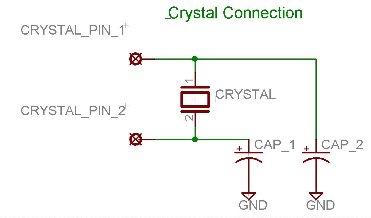
- PIN 13: OSC1/CLKIN: This is the oscillator input or the external clock input pin.
- PIN 14: OSC2/CLKOUT: This is the oscillator output pin. A crystal resonator is connected between pin 13 and 14 to provide external clock to the microcontroller. ¼ of the frequency of OSC1 is outputted by OSC2 in case of RC mode. This indicates the instruction cycle rate.
- PIN 15: RC0/T1OCO/T1CKI: PORTC consists of 8 pins. It is also a bidirectional input output port. Of them, pin 15 is the first. It can be the clock input of timer 1 or the oscillator output of timer 2.
- PIN 16: RC1/T1OSI/CCP2: It can be the oscillator input of timer 1 or the capture 2 input/compare 2 output/ PWM 2 output.
- PIN 17: RC2/CCP1: It can be the capture 1 input/ compare 1 output/ PWM 1 output.
- PIN 18: RC3/SCK/SCL: It can be the output for SPI or I2C modes and can be the input/output for synchronous serial clock.
- PIN 23: RC4/SDI/SDA: It can be the SPI data in pin. Or in I2C mode it can be data input/output pin.
- PIN 24: RC5/SDO: It can be the data out of SPI in the SPI mode.
- PIN 25: RC6/TX/CK: It can be the synchronous clock or USART Asynchronous transmit pin.
- PIN 26: RC7/RX/DT: It can be the synchronous data pin or the USART receive pin.
- PIN 19,20,21,22,27,28,29,30: All of these pins belong to PORTD which is again a bidirectional input and output port. When the microprocessor bus is to be interfaced, it can act as the parallel slave port.
- PIN 33-40: PORT B: All these pins belong to PORTB. Out of which RB0 can be used as the external interrupt pin and RB6 and RB7 can be used as in-circuit debugger pins.


